VIAs
- Home
- Capabilities
- VIAs
VIAs
| Property | |
| Through vias | |
| Blind vias | |
| BLIND VIA - Min. hole | 0,1 mm |
| BLIND VIA - Min. outerlayer pad | 0,3 mm |
| BLIND VIA - Min. innerlayer pad | 0,3 mm |
| BLIND VIA - Aspect ratio (hole depth : hole diameter) | 1:1 |
| BLIND VIA - Filled | Non conductive resin |
| Buried vias | |
| Stacked vias | |
| Staggered vias | |
| Plugged vias |
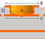
Blind vias
Min. drilled hole = A = 0,1mm
Min. outerlayer pad = B = 0,3mm
Min. innerlayer pad = C = 0,3mm
Aspect ratio = D:A = 1:1
Min. outerlayer pad = B = 0,3mm
Min. innerlayer pad = C = 0,3mm
Aspect ratio = D:A = 1:1
Combination of hidden and blind vias
If blind and hidden vias are present as a combination, please contact PCB Baltic to get the current capability, since other properties of the pcb can affect final suggestions.

Filled blind vias
If blind vias are located in SMD pads, we can provide filled blind vias to get a flat surface. This would help to make the layout more compact and to use a BGA solderpad as a via pad for routing signal to inner layer.

Stacked vias
If via size is small and not possible to drill thicker dielectric through, stacked vias can be uesed (microvia stacked on microvia).
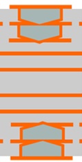
Staggered vias
Staggered vias = stacked vias with offset center


Quality
We are checking all orders according to our quality control program, regardless of volume or lead time.

Quick turn around prototypes service
We launched MULTI-PANEL service, so we can offer costs effective solution to our customers.

Focus on small-medium series
PCB Baltic is an innovative company with wide range of technology and team of experienced engineers.

Delivery on time everytime
A few hours is often of the utmost importance. We know the value of in time deliveries. PCB Baltic company has a well known reputation for precise deliveries.